- 您现在的位置:买卖IC网 > Sheet目录307 > ADP3611JRMZ-REEL (ON Semiconductor)IC MOSFET DRIVER DUAL 10-MSOP
�� �
�
�ADP3611�
�polarity� reversal� of� the� inductor� current� to� maximize� light�
�load� conversion� efficiency.� DRVLSD� can� also� be� pulled�
�low� for� reverse� voltage� protection� purposes.�
�When� DRVLSD� is� low,� the� low-side� driver� stays� low.�
�When� DRVLSD� is� high,� the� low-side� driver� is� enabled� and�
�controlled� by� the� driver� signals,� as� previously� described.�
�Low� ?� Side� Driver� Timeout�
�In� normal� operation,� the� DRVH� signal� tracks� the� IN�
�signal� and� turns� off� the� Q1� high-side� switch� with� a� few� 10�
�ns� delay� (t� pdlDRVH� )� following� the� falling� edge� of� the� input�
�signal.� When� Q1� is� turned� off,� DRVL� is� allowed� to� go� high,�
�Q2� turns� on,� and� the� SW� node� voltage� collapses� to� zero.� But�
�in� a� fault� condition� such� as� a� high-side� Q1� switch�
�drain-source� short� circuit,� the� SW� node� cannot� fall� to� zero,�
�Crowbar� Function�
�In� addition� to� the� internal� low-side� drive� time-out� circuit,�
�the� ADP3611� includes� a� CROWBAR� input� pin� to� provide�
�a� means� for� additional� overvoltage� protection.� When�
�CROWBAR� goes� high,� the� ADP3611� turns� off� DRVH� and�
�turns� on� DRVL.� The� crowbar� logic� overrides� the� overlap�
�protection� circuit,� the� shutdown� logic,� the� DRVLSD� logic,�
�and� the� UVLO� protection� on� DRVL.� Thus,� the� crowbar�
�function� maximizes� the� overvoltage� protection� coverage� in�
�the� application.� The� CROWBAR� can� be� either� driven� by�
�the� CLAMP� pin� of� buck� controllers,� such� as� the�
�ADP3207A,� or� ADP3210,� or� controlled� by� an� independent�
�overvoltage� monitoring� circuit.�
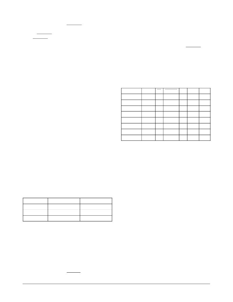
�Table� 5.� ADP3611� Truth� Table�
�even� when� DRVH� goes� low.� The� ADP3611� has� a� timer�
�circuit� to� address� this� scenario.� Every� time� the� IN� goes� low,�
�a� DRVL� on-time� delay� timer� is� triggered.� If� the� SW� node�
�voltage� does� not� trigger� a� low-side� turn-on,� the� DRVL�
�on-time� delay� circuit� does� it� instead,� when� it� times� out� with�
�t� SW(TO)� delay.� If� Q1� is� still� turned� on,� that� is,� its� drain� is�
�shorted� to� the� source,� Q2� turns� on� and� creates� a� direct� short�
�circuit� across� the� V� DCIN� voltage� rail.� The� crowbar� action�
�causes� the� fuse� in� the� V� DCIN� current� path� to� open.� The�
�opening� of� the� fuse� saves� the� load� (CPU)� from� potential�
�damage� that� the� high-side� switch� short� circuit� could� have�
�caused.�
�CROWBAR�
�L�
�L�
�L�
�L�
�L�
�L�
�H�
�H�
�UVLO�
�L�
�L�
�L�
�L�
�L�
�H�
�L�
�H�
�SD�
�H�
�H�
�H�
�H�
�L�
�*�
�*�
�*�
�DRVLSD�
�H�
�H�
�L�
�L�
�*�
�*�
�*�
�*�
�IN�
�H�
�L�
�H�
�L�
�*�
�*�
�*�
�*�
�DRVH�
�H�
�L�
�H�
�L�
�L�
�L�
�L�
�L�
�DRVL�
�L�
�H�
�L�
�L�
�L�
�L�
�H�
�H�
�*� =� Don’t� Care�
�APPLICATION� INFORMATION�
�Supply� Capacitor� Selection�
�For� the� supply� input� (VCC)� of� the� ADP3611,� a� local�
�bypass� capacitor� is� recommended� to� reduce� the� noise� and�
�to� supply� some� of� the� peak� currents� drawn.� Use� a� 10� m� F� or�
�4.7� m� F� multilayer� ceramic� (MLC)� capacitor.� MLC�
�capacitors� provide� the� best� combination� of� low� ESR� and�
�small� size,� and� can� be� obtained� from� the� following� vendors.�
�Table� 6.�
�where:�
�Q� HSGATE� is� the� total� gate� charge� of� the� high-side� MOSFET.�
�D� V� BST� is� the� voltage� droop� allowed� on� the� high-side�
�MOSFET� drive.�
�For� example,� two� NTMFS4821N� MOSFETs� in� parallel�
�have� a� total� gate� charge� of� about� 20� nC.� For� an� allowed�
�droop� of� 100� mV,� the� required� bootstrap� capacitance� is�
�200� nF.� A� good� quality� ceramic� capacitor� should� be� used,�
�Vendor�
�Murata�
�Taiyo� ?� Yuden�
�Part� Number�
�GRM235Y5V106Z16�
�EMK325F106ZF�
�Web� Address�
�www.murata.com�
�www.t� ?� yuden.com�
�and� derating� for� the� significant� capacitance� drop� of� MLCs�
�at� high� temperature� must� be� applied.� In� this� example,�
�selection� of� 470� nF� or� even� 1� m� F� would� be� recommended.�
�Normally� a� Schottky� diode� is� recommended� for� the�
�Tokin� C23Y5V1C106ZP� www.tokin.com�
�Keep� the� ceramic� capacitor� as� close� as� possible� to� the� ADP3611.�
�Bootstrap� Circuit�
�The� bootstrap� circuit� uses� a� charge� storage� capacitor�
�(CBST)� and� a� synchronous� MOSFET� rectifier� (D1),� as�
�shown� in� Figure� 18.� Selection� of� these� components� can� be�
�done� after� the� high-side� MOSFET� has� been� chosen.� The�
�bootstrap� capacitor� must� have� a� voltage� rating� that� is� able�
�to� handle� at� least� 5� V� more� than� the� maximum� supply�
�bootstrap� diode� due� to� its� low� forward� drop,� which�
�maximizes� the� drive� available� for� the� high-side� MOSFET.�
�Using� a� synchronous� MOSFET� rectifier� instead� of� a�
�Schottky� diode� has� the� advantage� of� an� even� lower� forward�
�voltage� drop.� A� lower� forward� voltage� drop� gives� a� larger�
�drive� voltage� for� the� high-side� MOSFET� and� a� lower�
�conduction� loss� for� the� high-side� MOSFET.� The� bootstrap�
�diode� must� also� be� able� to� handle� at� least� 5� V� more� than� the�
�maximum� battery� voltage.� The� average� forward� current�
�can� be� estimated� by�
�Q� HSGATE�
�D� V� BST�
�voltage.� The� capacitance� is� determined� by�
�C� BST� +�
�(eq.� 1)�
�I� F(AVG)� +� Q� HSGATE� f� MAX� (eq.� 2)�
�where� f� MAX� is� the� maximum� switching� frequency� of� the�
�controller.�
�http://onsemi.com�
�10�
�发布紧急采购,3分钟左右您将得到回复。
相关PDF资料
ADP5501ACPZ-RL
IC LED DRVR WHITE BCKLGT 24LFCSP
ADP8863ACPZ-R7
IC LED DRVR WHIT BCKLGT 20-WLCSP
ADUM1100UR
IC DIGITAL ISOL/COUPLER 8SOIC
ADUM1201CR
IC ISOLATOR DIGITAL DUAL 8SOIC
ADUM1210BRZ
IC ISOLATOR DIGITAL DUAL 8SOIC
ADUM1233BRWZ-RL
IC ISOLATR DGTL 2CH 0.1A 16-SOIC
ADUM1234BRWZ-RL
IC ISOLATR DGTL 2CH 0.1A 16-SOIC
ADUM1250SRZ-RL7
IC ISOLATOR 1MBPS 4CH 2.5K 8SOIC
相关代理商/技术参数
ADP3611MNR2G
功能描述:功率驱动器IC DUAL HI VOLT MOSFET RoHS:否 制造商:Micrel 产品:MOSFET Gate Drivers 类型:Low Cost High or Low Side MOSFET Driver 上升时间: 下降时间: 电源电压-最大:30 V 电源电压-最小:2.75 V 电源电流: 最大功率耗散: 最大工作温度:+ 85 C 安装风格:SMD/SMT 封装 / 箱体:SOIC-8 封装:Tube
ADP3611MNR2G-REEL
制造商:ONSEMI 制造商全称:ON Semiconductor 功能描述:Dual Bootstrapped, High Voltage MOSFET Driver with Output Disable
ADP3623
制造商:AD 制造商全称:Analog Devices 功能描述:High Speed, Dual, 4 A MOSFET Driver with Thermal Protection
ADP3623ARDZ-RL
功能描述:IC MOSFET DVR 4A DL HS 8SOIC RoHS:是 类别:集成电路 (IC) >> PMIC - MOSFET,电桥驱动器 - 外部开关 系列:- 标准包装:95 系列:- 配置:高端和低端,独立 输入类型:非反相 延迟时间:160ns 电流 - 峰:290mA 配置数:1 输出数:2 高端电压 - 最大(自引导启动):600V 电源电压:10 V ~ 20 V 工作温度:-40°C ~ 125°C 安装类型:表面贴装 封装/外壳:8-SOIC(0.154",3.90mm 宽) 供应商设备封装:8-SOIC 包装:管件 产品目录页面:1381 (CN2011-ZH PDF)
ADP3623ARHZ-RL
功能描述:IC MOSFET DVR 4A DL HS 8MSOP RoHS:是 类别:集成电路 (IC) >> PMIC - MOSFET,电桥驱动器 - 外部开关 系列:- 标准包装:95 系列:- 配置:高端和低端,独立 输入类型:非反相 延迟时间:160ns 电流 - 峰:290mA 配置数:1 输出数:2 高端电压 - 最大(自引导启动):600V 电源电压:10 V ~ 20 V 工作温度:-40°C ~ 125°C 安装类型:表面贴装 封装/外壳:8-SOIC(0.154",3.90mm 宽) 供应商设备封装:8-SOIC 包装:管件 产品目录页面:1381 (CN2011-ZH PDF)
ADP3624
制造商:AD 制造商全称:Analog Devices 功能描述:High Speed, Dual, 4 A MOSFET Driver with Thermal Protection
ADP3624ARDZ
功能描述:IC DRIVER DUAL 4A NONINV 8SOIC RoHS:是 类别:集成电路 (IC) >> PMIC - MOSFET,电桥驱动器 - 外部开关 系列:- 标准包装:95 系列:- 配置:半桥 输入类型:PWM 延迟时间:25ns 电流 - 峰:1.6A 配置数:1 输出数:2 高端电压 - 最大(自引导启动):118V 电源电压:9 V ~ 14 V 工作温度:-40°C ~ 125°C 安装类型:表面贴装 封装/外壳:8-SOIC(0.154",3.90mm 宽) 供应商设备封装:8-SOIC 包装:管件 产品目录页面:1282 (CN2011-ZH PDF) 其它名称:*LM5104M*LM5104M/NOPBLM5104M
ADP3624ARDZ-RL
功能描述:IC DVR DUAL NONINVERT 4A 8SOIC RoHS:是 类别:集成电路 (IC) >> PMIC - MOSFET,电桥驱动器 - 外部开关 系列:- 标准包装:50 系列:- 配置:低端 输入类型:非反相 延迟时间:40ns 电流 - 峰:9A 配置数:1 输出数:1 高端电压 - 最大(自引导启动):- 电源电压:4.5 V ~ 35 V 工作温度:-40°C ~ 125°C 安装类型:表面贴装 封装/外壳:TO-263-6,D²Pak(5 引线+接片),TO-263BA 供应商设备封装:TO-263 包装:管件